
Featured article
Advanced Deep Learning Techniques Explained
Covers advanced deep learning techniques, including core methods, real-world applications, implementation challenges, and risks for practitioners.
Open notes for practical knowledge
A Wikipedia-style knowledge blog with practical guides, reference articles, and structured research notes.
Covers advanced deep learning techniques, including core methods, real-world applications, implementation challenges, and risks for practitioners.
Covers advanced deep learning techniques, including core methods, real-world applications, implementation challenges, and risks for practitioners.

Explores how artificial intelligence shapes continuity and uninterrupted service, covering practical use cases, benefits, limitations, and risks.
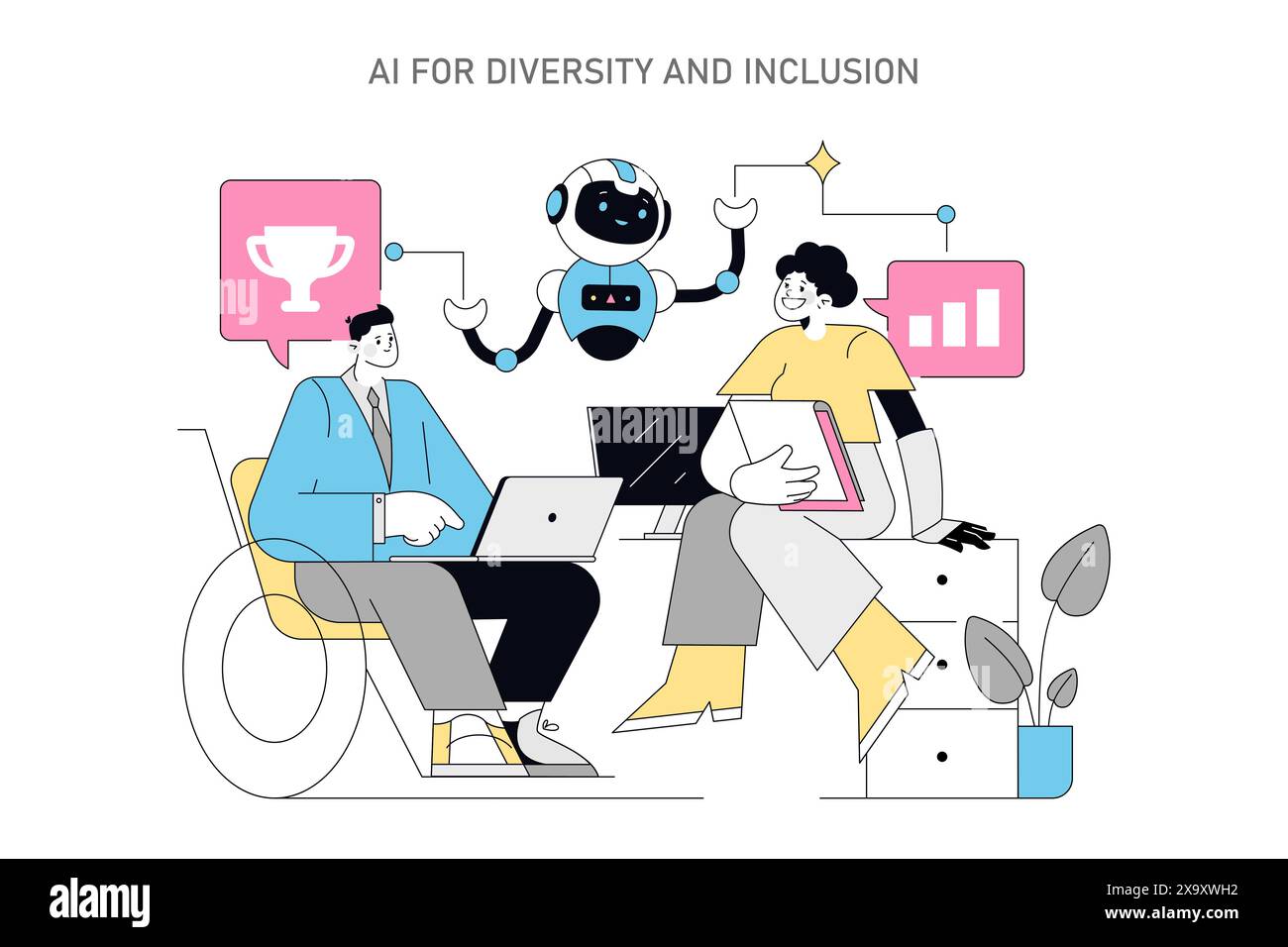
Explores how artificial intelligence shapes diversity and promoting inclusion, covering practical use cases, benefits, limitations, and risks.

Explores how artificial intelligence shapes IoT and smart devices, covering practical use cases, benefits, limitations, and risks.
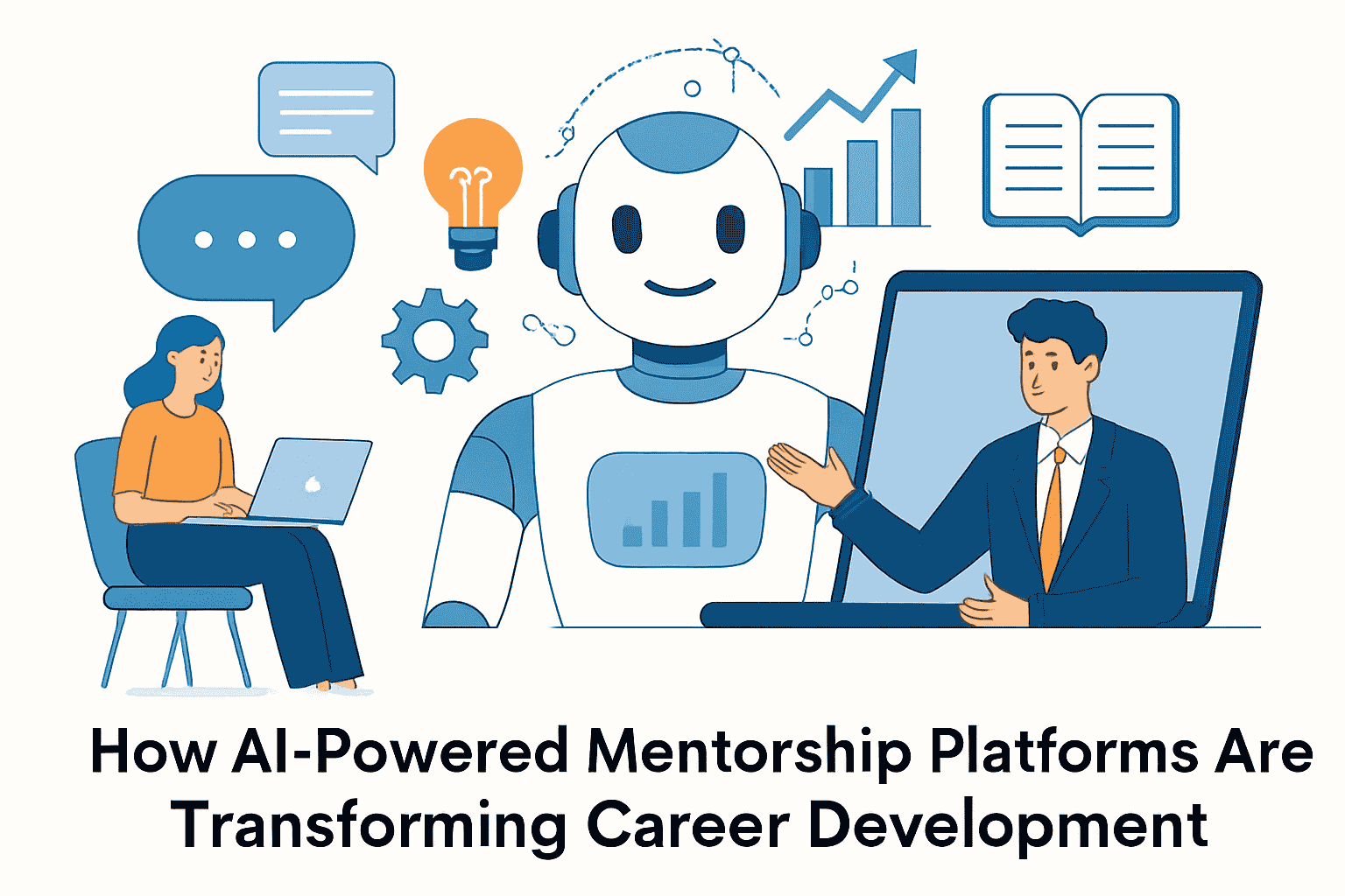
Explores how artificial intelligence shapes mentorship and learning from experts, covering practical use cases, benefits, limitations, and risks.

Explores how artificial intelligence shapes online learning and accessible education, covering practical use cases, benefits, limitations, and risks.